Winbond SDRAM LPDDR móvil W949D2DBJX5I, 512 MB, Superficie, VFBGA 32 bit, 90 pines
- Código RS:
- 188-2651
- Referência do fabricante:
- W949D2DBJX5I
- Fabricante:
- Winbond

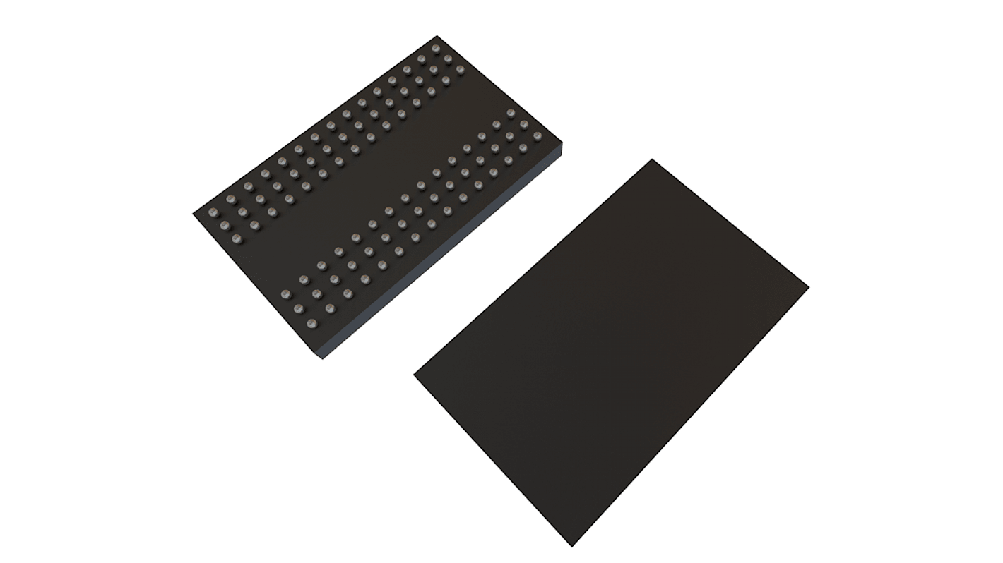
A imagem representada pode não ser a do produto
Informação de stock atualmente indisponível
- Código RS:
- 188-2651
- Referência do fabricante:
- W949D2DBJX5I
- Fabricante:
- Winbond
Especificações
Documentação Técnica
Legislação e Conformidade
Detalhes do produto
Seleciona um o mais atributos para encontrar produtos semelhantes.
Selecionar tudo | Atributo | Valor |
|---|---|---|
| Marca | Winbond | |
| Tipo de producto | SDRAM LPDDR móvil | |
| Tamaño de la memoria | 512MB | |
| Ancho del bus de datos | 32bit | |
| Número de líneas de bus | 15bit | |
| Número de bits por palabra | 8 | |
| Frecuencia del reloj máxima | 200MHZ | |
| Tiempo de acceso aleatorio máximo | 5ns | |
| Número de palabras | 64M | |
| Tipo de montaje | Superficie | |
| Encapsulado | VFBGA | |
| Número de pines | 90 | |
| Temperatura de Funcionamiento Mínima | -40°C | |
| Temperatura de funcionamiento máxima | 85°C | |
| Altura | 0.65mm | |
| Certificaciones y estándares | LVCMOS Compatible | |
| Serie | W949D2DB | |
| Longitud | 13.1mm | |
| Tensión de alimentación mínima | 1.7V | |
| Tensión de alimentación máxima | 1.95V | |
| Estándar de automoción | No | |
| Selecionar tudo | ||
|---|---|---|
Marca Winbond | ||
Tipo de producto SDRAM LPDDR móvil | ||
Tamaño de la memoria 512MB | ||
Ancho del bus de datos 32bit | ||
Número de líneas de bus 15bit | ||
Número de bits por palabra 8 | ||
Frecuencia del reloj máxima 200MHZ | ||
Tiempo de acceso aleatorio máximo 5ns | ||
Número de palabras 64M | ||
Tipo de montaje Superficie | ||
Encapsulado VFBGA | ||
Número de pines 90 | ||
Temperatura de Funcionamiento Mínima -40°C | ||
Temperatura de funcionamiento máxima 85°C | ||
Altura 0.65mm | ||
Certificaciones y estándares LVCMOS Compatible | ||
Serie W949D2DB | ||
Longitud 13.1mm | ||
Tensión de alimentación mínima 1.7V | ||
Tensión de alimentación máxima 1.95V | ||
Estándar de automoción No | ||
VDD = 1.7∼1.95V
VDDQ = 1.7∼1.95V
Data width: x16 / x32
Clock rate: 200MHz (-5),166MHz (-6)
Standard Self Refresh Mode
Partial Array Self-Refresh(PASR)
Auto Temperature Compensated Self Refresh (ATCSR)
Power Down Mode
Deep Power Down Mode (DPD Mode)
Programmable output buffer driver strength
Four internal banks for concurrent operation
Data mask (DM) for write data
Clock Stop capability during idle periods
Auto Pre-charge option for each burst access
Double data rate for data output
Differential clock inputs (CK and CK)
Bidirectional, data strobe (DQS)
CAS Latency: 2 and 3
Burst Length: 2, 4, 8 and 16
Burst Type: Sequential or Interleave
8K refresh cycles/64 mS
Interface: LVCMOS compatible
Support package:
60 balls VFBGA (x16)
90 balls VFBGA (x32)
Operating Temperature Range
Extended: -25°C ≤ TCASE ≤ 85°C
Industrial: -40°C ≤ TCASE ≤ 85°C
This is a 512Mb Low Power DDR SDRAM organized as 2M words x 4 banks x 32bits.
Burst Type: Sequential or Interleave
Standard Self Refresh Mode
PASR, ATCSR, Power Down Mode、DPD
Programmable output buffer driver strength
Four internal banks for concurrent operation
Bidirectional, data strobe (DQS) is transmitted or received with data, to be used in capturing data at the receiver
Links relacionados
- Winbond SDRAM LPDDR móvil, 512 MB, Superficie, VFBGA 32 bit, 90 pines
- Winbond SDRAM LPDDR móvil, 512 MB, Superficie, VFBGA 16 bit, 60 pines
- Winbond SDRAM LPDDR móvil W949D6DBHX5I, 512 MB, Superficie, VFBGA 16 bit, 60 pines
- Winbond SDRAM, 512 MB, Superficie, VFBGA 16 bit, 84 pines
- Winbond SDRAM W9751G6NB25I, 512 MB, Superficie, VFBGA 16 bit, 84 pines
- Winbond SDRAM, 1 Gb, Superficie, VFBGA 16 bit, 78 pines
- Winbond SDRAM, 1 Gb, Superficie, VFBGA 16 bit, 60 pines
- Winbond SDRAM, 1 Gb, Superficie, VFBGA 16 bit, 96 pines