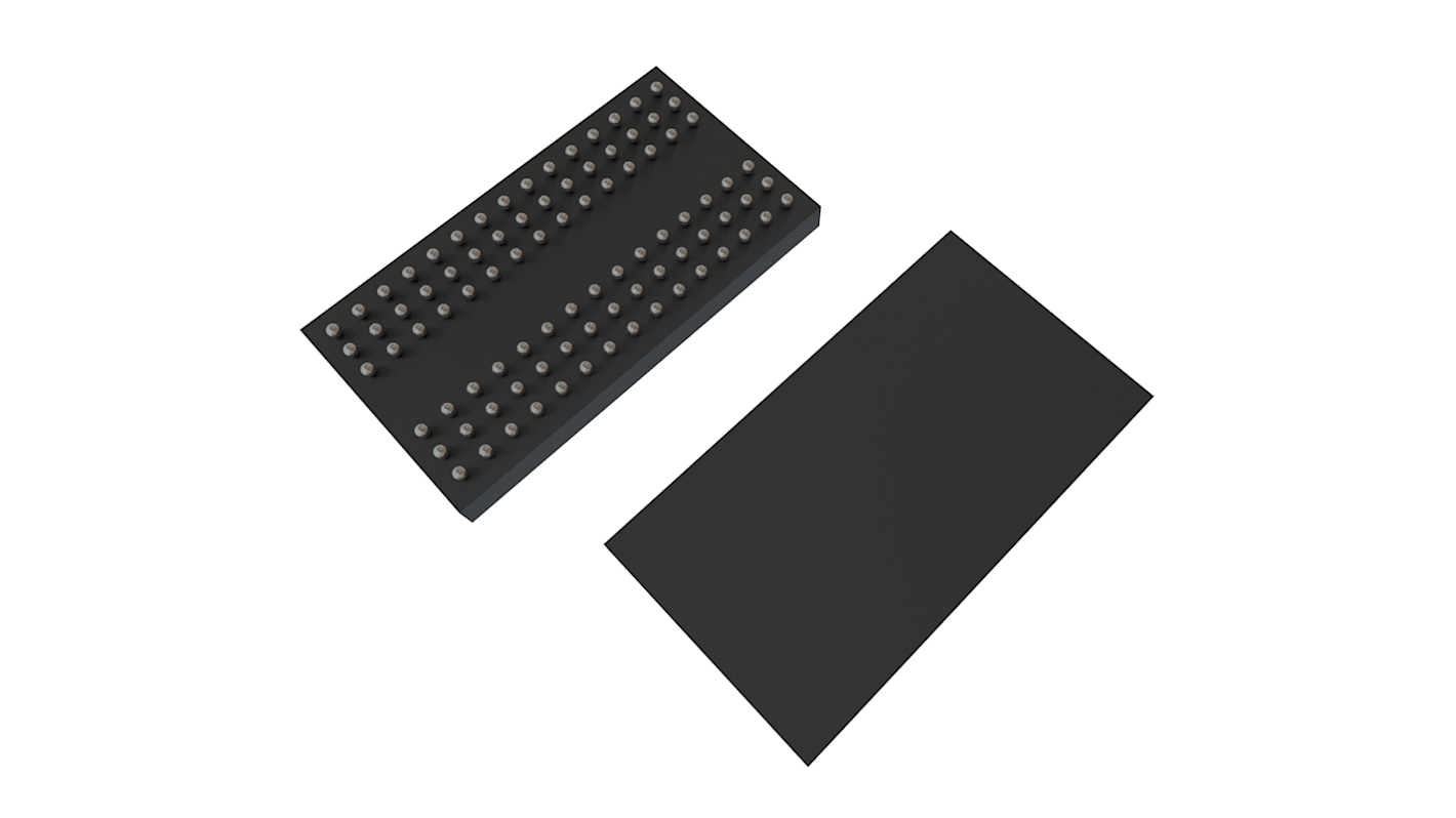
SDRAM W9712G6KB25I, 128Mbit, 200MHZ, Montaje superficial, TFBGA, 84 pines DDR2

- Código RS:
- 188-2730P
- Referência do fabricante:
- W9712G6KB25I
- Fabricante:
- Winbond
Temporariamente fora de stock. Disponível a 02/12/2024, com entrega em 4 dia(s) útil(eis).
Adicionado
Preço Unidade (fornecido em bandeja)
1,904 €
| Unidades | Por unidade |
| 10 - 15 | 1,904 € |
| 20 - 45 | 1,87 € |
| 50 - 95 | 1,846 € |
| 100 + | 1,658 € |
- Código RS:
- 188-2730P
- Referência do fabricante:
- W9712G6KB25I
- Fabricante:
- Winbond
Documentação Técnica
Legislação e Conformidade
- COO (País de Origem):
- TW
Detalhes do produto
The W9712G6KB is a 128M bits DDR2 SDRAM and speed involving -25, 25I and -3.
Double Data Rate architecture: two data transfers per clock cycle
CAS Latency: 3, 4, 5 and 6
Burst Length: 4 and 8
Bi-directional, differential data strobes (DQS and /DQS ) are transmitted / received with data
Edge-aligned with Read data and center-aligned with Write data
DLL aligns DQ and DQS transitions with clock
Differential clock inputs (CLK and /CLK)
Data masks (DM) for write data
Commands entered on each positive CLK edge, data and data mask are referenced to both edges of /DQS
Posted /CAS programmable additive latency supported to make command and data bus efficiency
Read Latency = Additive Latency plus CAS Latency (RL = AL + CL)
Off-Chip-Driver impedance adjustment (OCD) and On-Die-Termination (ODT) for better signal quality
Auto-precharge operation for read and write bursts
Auto Refresh and Self Refresh modes
Precharged Power Down and Active Power Down
Write Data Mask
Write Latency = Read Latency - 1 (WL = RL - 1)
Interface: SSTL_18
Especificações
Atributo | Valor |
|---|---|
| Tamaño de la Memoria | 128Mbit |
| Clase SDRAM | DDR2 |
| Organización | 16M x 8 bit |
| Transmisión de Datos | 200MHZ |
| Ancho del Bus de Datos | 16bit |
| Ancho del Bus de Direcciones | 15bit |
| Número de Bits de Palabra | 8bit |
| Tiempo de Acceso Aleatorio Máximo | 0.4ns |
| Número de Palabras | 16M |
| Tipo de Montaje | Montaje superficial |
| Tipo de Encapsulado | TFBGA |
| Conteo de Pines | 84 |
| Dimensiones | 12.6 x 8.1 x 0.8mm |
| Altura | 0.8mm |
| Longitud | 12.6mm |
| Temperatura Máxima de Funcionamiento | +95 °C |
| Tensión de Alimentación de Funcionamiento Mínima | 1.7 V |
| Ancho | 8.1mm |
| Temperatura de Funcionamiento Mínima | -40 °C |
| Tensión de Alimentación Máxima de Funcionamiento | 1.9 V |